
Design of ALU
ALU or Arithmetic Logical Unit is a digital circuit to do arithmetic operations like addition, subtraction,division, multiplication and logical oparations like and, or, xor, nand, nor etc. A simple block diagram of a 4 bit ALU for operations and,or,xor and Add is shown here :
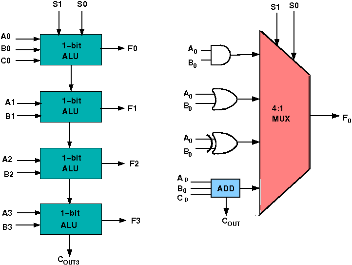
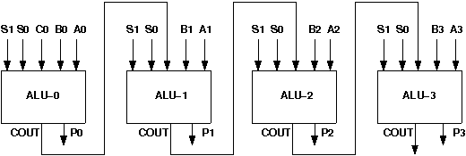
The 4-bit ALU block is combined using 4 1-bit ALU block
Design Issues :
The circuit functionality of a 1 bit ALU is shown here, depending upon the control signal S1 and S0 the circuit operates as follows:
for Control signal S1 = 0 , S0 = 0, the output is A And B,
for Control signal S1 = 0 , S0 = 1, the output is A Or B,
for Control signal S1 = 1 , S0 = 0, the output is A Xor B,
for Control signal S1 = 1 , S0 = 1, the output is A Add B.
The truth table for 16-bit ALU with capabilities similar to 74181 is shown here:
| Mode Select | Fn for active HIGH operands | ||||
|---|---|---|---|---|---|
| Inputs | Logic | Arithmetic (note 2) | |||
| S3 | S2 | S1 | S0 | (M = H) | (M = L) (Cn=L) |
| L | L | L | L | A' | A |
| L | L | L | H | A'+B' | A+B |
| L | L | H | L | A'B | A+B' |
| L | L | H | H | Logic 0 | minus 1 |
| L | H | L | L | (AB)' | A plus AB' |
| L | H | L | H | B' | (A + B) plus AB' |
| L | H | H | L | A ⊕ B | A minus B minus 1 |
| L | H | H | H | AB' | AB minus 1 |
| H | L | L | L | A'+B | A plus AB |
| H | L | L | H | (A ⊕ B)' | A plus B |
| H | L | H | L | B | (A + B') plus AB |
| H | L | H | H | AB | AB minus 1 |
| H | H | L | L | Logic 1 | A plus A (Note 1) |
| H | H | L | H | A+B' | (A + B) plus A |
| H | H | H | L | A+B | (A + B') plus A |
| H | H | H | H | A | A minus 1 |
The L denotes the logic low and H denotes logic high.

Objective of 4 bit arithmetic logic unit (with AND, OR, XOR, ADD operation):
- Understanding behaviour of arithmetic logic unit from working module and the module designed by the student as part of the experiment
- Designing an arithmetic logic unit for given parameter
Examining behaviour of arithmetic logic unit for the working module and module designed by the student as part of the experiment (refer to the circuit diagram):
Loading data in the arithmetic logic unit (refer to procedure tab for further detail and experiment manual for pin numbers):
- load the two input numbers as:
- A(A3 A2 A1 A0): A3=1, A2=1, A1=0, A0=0
- B(B3 B2 B1 B0): B3=1, B2=0, B1=0, B0=1
- carry in(C0)=0
examining the AND behaviour:
- load data in select input as:
- S1=0, S0=0 `
- check output:
- F3=1, F2=0, F1=0, F0=0
- cout=0 `
examining the OR behaviour:
- load data in select input as:
- S1=0, S0=1 `
- check output:
- F3=1, F2=1, F1=0, F0=1
- cout=0 `
examining the XOR behaviour:
- load data in select input as:
- S1=1, S0=0 `
- check output:
- F3=0, F2=1, F1=0, F0=1
- cout=0 `
examining the ADD behaviour:
- load data in select input as:
- S1=1, S0=1 `
- check output:
- F3=0, F2=1, F1=0, F0=1
- cout=1 `
Recommended learning activities for the experiment: Leaning activities are designed in two stages, a basic stage and an advanced stage. Accomplishment of each stage can be self-evaluated through the given set of quiz questions consisting of multiple type and subjective type questions. In the basic stage, it is recommended to perform the experiment firstly, on the given encapsulated working module, secondly, on the module designed by the student, having gone through the theory, objective and procuder. By performing the experiment on the working module, students can only observe the input-output behavior. Where as, performing experiments on the designed module, students can do circuit analysis, error analysis in addition with the input-output behavior. It is recommended to perform the experiments following the given guideline to check behavior and test plans along with their own circuit analysis. Then students are recommended to move on to the advanced stage. The advanced stage includes the accomplishment of the given assignments which will provide deeper understanding of the topic with innovative circuit design experience. At any time, students can mature their knowledge base by further reading the references provided for the experiment.
- if value is UNKNOWN, wire color= maroon
- if value is TRUE, wire color= blue
- if value is FALSE, wire color= black
- if value is HI IMPEDENCE, wire color= green
- if value is INVALID, wire color= orange
likewise the 16 bit arithmetic logic unit can be designed and tested
- by cascading 4 bit ALUs only the carry will propagate to the next level for ADD operation
Test plan :
- Set inputs 0101 and 0011 and check output for all possible select input combinations.
- Set any two 16-bit number and check output for all possible select input combinations.
Use Display units for checking output. Try to use minimum number of components to build. The pin configuration of the canned components are shown when mouse hovered over a component.
Assignment Statements :
- Design a 4 bit ALU comprising only the AND, OR, XOR and Add operations.
- Design a 16-bit ALU with capabilities similar to 74181

Design of ALU:
To see the step by step process to perform the experiment in simulator follow tutorial
4-bit Slice ALU Tutorial
or follow the steps below.
- Start the simulator as directed.This simulator supports 5-valued logic.
- To design the circuit we need 4 1-bit ALU, 11 Bit switch (to give input,which will toggle its value with a double click), 5 Bit displays (for seeing output), wires.
- The pin configuration of a component is shown whenever the mouse is hovered on any canned component of the palette. Pin numbering starts from 1 and from the bottom left corner (indicating with the circle) and increases anticlockwise.
- For 1-bit ALU input A0 is in pin-9,B0 is in pin-10, C0 is in pin-11 (this is input carry), for selection of operation, S0 is in pin-12, S1 is in pin-13, output F is in pin-8 and output carry is pin-7
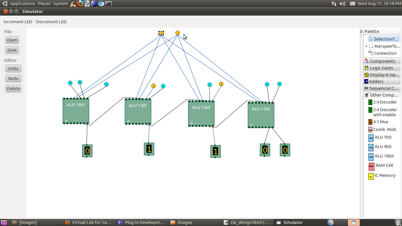
- Click on the 1-bit ALU component (in the Other Component drawer in the pallet) and then click on the position of the editor window where you want to add the component (no drag and drop, simple click will serve the purpose), likewise add 3 more 1-bit ALU (from the Other Component drawer in the pallet), 11 Bit switches and 5 Bit Displays (from Display and Input drawer of the pallet,if it is not seen scroll down in the drawer), 3 digital display and 1 bit Displays (from Display and Input drawer of the pallet,if it is not seen scroll down in the drawer)
- To connect any two components select the Connection menu of Palette, and then click on the Source terminal and click on the target terminal. According to the circuit diagram connect all the components. Connect the Bit switches with the inputs and Bit displays component with the outputs. After the connection is over click the selection tool in the pallete.
- See the output, in the screenshot diagram we have given the value of S1 S0=11 which will perform add operation and two number input as A0 A1 A2 A3=0010 and B0 B1 B2 B3=0100 so get output F0 F1 F2 F3=0110 as sum and 0 as carry which is indeed an add operation.you can also use many other combination of different values and check the result. The operations are implemented using the truth table for 4 bit ALU given in the theory.
Circuit diagram of 4 bit ALU:
Screenshot of Design of 4 bit ALU:
Components :
To build any 4 bit ALU, we need :
- AND gate, OR gate, XOR gate
- Full Adder,
- 4-to-1 MUX<
- Wires to connect.
In case of counters the number of flip-flops depends on the number of different states in the counter.

Design of ALU :
General guideline to use the simulator for performing the experiment:
- Start the simulator as directed. For more detail please refer to the manual for using the simulator
- The simulator supports 5-valued logic
- To add the logic components to the editor or canvas (where you build the circuit) select any component and click on the position of the canvas where you want to add the component
- The pin configuration is shown when you select the component and press the 'show pinconfig' button in the left toolbar or whenever the mouse is hovered on any canned component of palette
- To connect any two components select the connection tool of palette, and then click on the source terminal and then click on the the target terminal
- To move any component select the component using the selection tool and drag the component to the desired position
- To give a toggle input to the circuit, use 'Bit Switch' which will toggle its value with a double click
- Use 'Bit Display' component to see any single bit value. 'Digital Display' will show the output in digital format
- undo/redo, delete, zoom in/zoom out, and other functionalities have been given in the top toolbar for ease of circuit building
- Use start/stop clock pulse to start or stop the clock input of the circuit. Clock period can be set from the given 'set clock' button in the left toolbar
- Use 'plot graph' button to see input-output wave forms
- Users can save their circuits with .logic extension and reuse them
- After building the circuit press the simulate button in the top toolbar to get the output
- If the circuit contains a clock pulse input, then the 'start clock' button will start the simulation of the whole circuit. Then there is no need to again press the 'simulate' button
Software for conducting the experiment, as appropriate for your platform, may be downloaded via SOFTWARE
General guideline to use the Simulator Software for performing the experiments:
- Windows (64 bit)
- Java runtime environment is needed (may get from java.com)
- Install downloaded jre
- Right click on My Computer/This PC
- Select Properties
- Select Advanced System Settings
- Select Advanced tab
- Select Environment Variables
- Select Path under System Variables
- Click on Edit button
- In Variable value editor paste this at the start of the line
C:\Program Files\Java\< jdk_version >\bin; - Click Ok then Ok again
- Linux (64 bit)
- If you are using linux platform then click on links under 'Linux(32 bit)' or if you are using then click on links under 'Windows(32 bit)' to download the Simulator Software
- Linux(32 bit)
- Windows(32 bit)
Click here to download the 64 bit version of simulator
PATH needs to be set:
If your environment is properly set up, you may open by double clicking on the jar file, otherwise use the following command:
java -jar coldvl64Windows.jar
Click here to download the 64 bit version of simulator
Once the simulator is downloaded, open the command prompt, then go to the directory where you have saved it using cd command and then give the following command to run the simulator:
java -jar coldvl64Linux.jar
Click here to download the new version of simulator
Once the simulator is downloaded, open the command prompt, then go to the directory where you have saved it using cd command and then give the following command to run the simulator:
java -jar coaSimulatorNew.jar
Click here to download the new version of simulator
Once the simulator is downloaded, open the command prompt, then go to the directory where you have saved it using cd command and then give the following command to run the simulator:
java -jar SimulatorNew.jar

You can download the Manuals from below mentioned links

Design of ALU :
Basic stage
Multiple choice questions:
- Maximum number of inputs to a data selector having 3 control pins
- How many 3 to 8 line decoders are required for a 1-of-32 decoder?
- What is the minimum number of two input NAND gates used to perform the function of two input OR gate ?
- A controlled inverter gives the 1's complement of the input
- The number of canonical expressions that can be developed over a 3-valued boolean algebra is
- A switching function is symmetric with respect to a set of literals if and only if the function remains unchanged after
3
8
4
9
8
1
4
2
2
4
3
5
True
False
16
32
64
8
Any permutation of the literals
All the literals are changed in clockwise order
Two of these literals are interchanged
All the literals are changed in anticlockwise order
Subjective questions:
- What does the selector inputs to an arithmetic logic unit (ALU) determine?
- How to design 16-bit ALU using 4-bit ALU?
Advanced stage
Multiple choice questions:
- Both the ALU and control unit of CPU employ special purpose storage which is called
- The number of levels in the design of a 64 X 1 mux using 4 X 1 mux
- On which factor the number of functions realized by a decoder depends?
- One mux can realize one function at a time and the functional dependency can be preseved in multilevel realizations
Registers
Buffers
Decoders
Multiplexers
4
5
3
2
Number of gates
Fanout capacity
Both
None of these
True
False
In 2's complement overflow
Can not occur when a positive value is added to a negative value
Is flagged whenever there is carry from sign bit addition
Is flagged when the carry from sign bit and previous bit matches
None of these
Subjective questions:
- Desig an ALU with one select variable s and two data inputs A and B. when s=0, the circuit performs addition operation F=A+B. when s=1, the circuit performs increment operation F=A+1
- Describe with a schematic diagram, how the ALU is connected to the processor registers through common bus.

Design of ALU :
References :
Books:
- Digital Logic and Computer Design - M. Morris Mano. Pearson Education - Prentice Hall.
- Computer Architecture and Organization - John P. Hayes
- Digital Principles Foundation of Circuit Design and Application - Arun Kumar Singh. New Age Publishers.
- The Art of Electronics - Paul Horowitz and Winfield Hill (1989). Cambridge University Press
- Modern Dictionary of Electronics - Rudolf F. Graf (1999). Newnes
Web Sites:
