
Design of Combinational Multipliers
Combinational Multipliers do multiplication of two unsigned binary numbers.Each bit of the multiplier is multiplied against the multiplicand, the product is aligned according to the position of the bit within the multiplier, and the resulting products are then summed to form the final result. Main advantage of binary multiplication is that the generation of intermediate products are simple: if the multiplier bit is a 1, the product is an appropriately shifted copy of the multiplicand; if the multiplier bit is a 0, the product is simply 0.
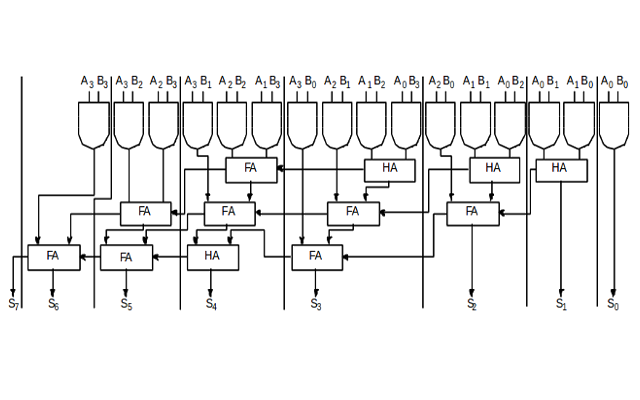
The design of a combinational multiplier to multiply two 4-bit binary number is illustrated below:
| A3 | A2 | A1 | A0 | ||||
| B3 | B2 | B1 | B0 | ||||
| A3 . B0 | A2 . B0 | A1 . B0 | A0 . B0 | ||||
| A3 . B1 | A2 . B1 | A1 . B1 | A0 . B1 | ||||
| A3 . B2 | A2 . B2 | A1 . B2 | A0 . B2 | ||||
| A3 . B3 | A2 . B3 | A1 . B3 | A0 . B3 | ||||
| S6 | S5 | S4 | S3 | S2 | S1 | S0 | |
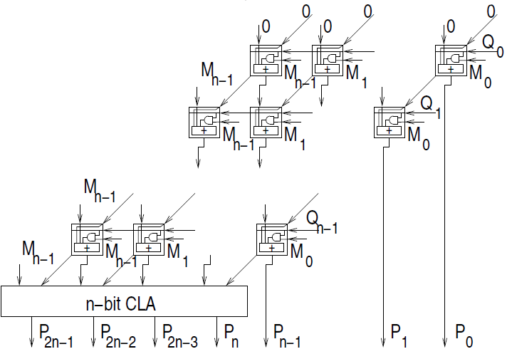
If two n-bit numbers are multiplied then the output will be less than or equals to 2n bits.
Some features of the multiplication scheme:
- it can be designed by unrolling the multiplier loop
- instead of handling the carry out of partial product summation bit,the carry out can be sent to the next bit of the next step
- this scheme of handling the carry is called carry save addition
- this scheme is more regular and modular
Logic diagram:

Objective of 4 bit carry lookahead adder:
To show that it is possible to construct a 4x4 combinational multiplier from an array of AND gates, half-adders and full-adders.
- understanding behaviour of combinational multiplier from module designed by the student as part of the experiment
- understanding the scheme implemented for the multiplication which is as follows (along with the logic diagram bellow):
- it can be designed by unrolling the multiplier loop
- instead of handling the carry out of partial product summation bit,the carry out can be sent to the next bit of the next step
- this scheme of handling the carry is called carry save addition
- The multiplier will multiply two 4 bit numbers
logic diagram:
Examining behaviour of combinational multiplier for the working module and module designed by the student as part of the experiment (refer to the circuit diagram)
Loading data in the combinational multiplier (refer to procedure tab for further detail and experiment manual for pin numbers)
- load the two input numbers as:
- multiplicand A (A3 A2 A1 A0): A3=1, A2=1, A1=0, A0=0
- multiplier B (B3 B2 B1 B0): B3=1, B2=0, B1=0, B0=1
Examining the behaviour:
- check output sum:
- sum (S7 S6 S5 S4 S3 S2 S1 S0): S7=0, S6=1, S5=1, S4=0, S3=1, S2=1, S1=0, S0=0
- at any level check how the carry propagates to the next level
- probing the carry port can be done by verifying the color of the wire coming out of the port
Recommended learning activities for the experiment: Leaning activities are designed in two stages, a basic stage and an advanced stage. Accomplishment of each stage can be self-evaluated through the given set of quiz questions consisting of multiple type and subjective type questions. In the basic stage, it is recommended to perform the experiment firstly, on the given encapsulated working module, secondly, on the module designed by the student, having gone through the theory, objective and procuder. By performing the experiment on the working module, students can only observe the input-output behavior. Where as, performing experiments on the designed module, students can do circuit analysis, error analysis in addition with the input-output behavior. It is recommended to perform the experiments following the given guideline to check behavior and test plans along with their own circuit analysis. Then students are recommended to move on to the advanced stage. The advanced stage includes the accomplishment of the given assignments which will provide deeper understanding of the topic with innovative circuit design experience. At any time, students can mature their knowledge base by further reading the references provided for the experiment.
- if value is UNKNOWN, wire color= maroon
- if value is TRUE, wire color= blue
- if value is FALSE, wire color= black
- if value is HI IMPEDENCE, wire color= green
- if value is INVALID, wire color= orange
Test plan :
- Set one input to zero(0) and check the output.
- Set one input to one(1) and check the output.
- Give proper inputs to check the identity, commutativity, associativity of multiplication operation with interchanging input values.
Use Display units for checking output. Try to use minimum number of components to build. The pin configuration of the canned components are shown when mouse hovered over a component.
Assignment Statements :
- Create a combinational multiplier circuit to multiply two 4-bit binary numbers. Use half adders, full adders and logic gates and test it by giving proper input.

Design of Combinational Multipliers :
Procedure to perform the experiment:Design of Combinational Multiplier
- Start the simulator as directed.This simulator supports 5-valued logic.
- To design the circuit we need 8 full adders, 4 half adders, 16 AND gates, 8 bit switch (to give input,which will toggle its value with a double click), 8 bit displays (to see the output), wires.
- The pin configuration of a component is shown whenever the mouse is hovered on any canned component of the palette or press the 'show pinconfig' button. Pin numbering starts from 1 and from the bottom left corner (indicated with the circle) and increases anticlockwise.
- For half adder input is in pin-5,8 output sum is in pin-4 and carry is pin-1, For full adder input is in pin-5,6,8 output sum is in pin-4 and carry is in pin-1
- Click on the half adder component (in the Adder drawer in the pallet) and then click on the position of the editor window where you want to add the component (no drag and drop, simple click will serve the purpose), likewise add 3 more half adders, 8 full adders (from the Adder drawer in the pallet), 16 AND gates (from Logic Gates drawer of the pallet,if it is not seen scroll down in the drawer), 8 Bit switches, 8 bit Displays (from Display and Input drawer of the pallet,if it is not seen scroll down in the drawer)
- To connect any two components select the Connection menu of Palette, and then click on the Source terminal and click on the target terminal. According to the circuit diagram connect all the components, connect bit switches to the input terminals. connect the output terminals to the Bit display component. After the connection is over click the selection tool in the pallete.
- See the output, bit switches are used to give input so that you can toggle its value with a double click and see the outputs with different inputs.
Circuit diagram of Combinational Multiplier:
Components :
To build a Combinational Multiplier, we need :
- 16 2-input AND Gates
- 4 half adders
- 8 full adders
- Display unit to show the outputs.
- Wires to connect.

Design of Combinational Multipliers :
General guideline to use the simulator for performing the experiment:
- Start the simulator as directed. For more detail please refer to the manual for using the simulator
- The simulator supports 5-valued logic
- To add the logic components to the editor or canvas (where you build the circuit) select any component and click on the position of the canvas where you want to add the component
- The pin configuration is shown when you select the component and press the 'show pinconfig' button in the left toolbar or whenever the mouse is hovered on any canned component of palette
- To connect any two components select the connection tool of palette, and then click on the source terminal and then click on the the target terminal
- To move any component select the component using the selection tool and drag the component to the desired position
- To give a toggle input to the circuit, use 'Bit Switch' which will toggle its value with a double click
- Use 'Bit Display' component to see any single bit value. 'Digital Display' will show the output in digital format
- undo/redo, delete, zoom in/zoom out, and other functionalities have been given in the top toolbar for ease of circuit building
- Use start/stop clock pulse to start or stop the clock input of the circuit. Clock period can be set from the given 'set clock' button in the left toolbar
- Use 'plot graph' button to see input-output wave forms
- Users can save their circuits with .logic extension and reuse them
- After building the circuit press the simulate button in the top toolbar to get the output
- If the circuit contains a clock pulse input, then the 'start clock' button will start the simulation of the whole circuit. Then there is no need to again press the 'simulate' button
Software for conducting the experiment, as appropriate for your platform, may be downloaded via SOFTWARE
General guideline to use the Simulator Software for performing the experiments:
- Windows (64 bit)
- Java runtime environment is needed (may get from java.com)
- Install downloaded jre
- Right click on My Computer/This PC
- Select Properties
- Select Advanced System Settings
- Select Advanced tab
- Select Environment Variables
- Select Path under System Variables
- Click on Edit button
- In Variable value editor paste this at the start of the line
C:\Program Files\Java\< jdk_version >\bin; - Click Ok then Ok again
- Linux (64 bit)
- If you are using linux platform then click on links under 'Linux(32 bit)' or if you are using then click on links under 'Windows(32 bit)' to download the Simulator Software
- Linux(32 bit)
- Windows(32 bit)
Click here to download the 64 bit version of simulator
PATH needs to be set:
If your environment is properly set up, you may open by double clicking on the jar file, otherwise use the following command:
java -jar coldvl64Windows.jar
Click here to download the 64 bit version of simulator
Once the simulator is downloaded, open the command prompt, then go to the directory where you have saved it using cd command and then give the following command to run the simulator:
java -jar coldvl64Linux.jar
Click here to download the new version of simulator
Once the simulator is downloaded, open the command prompt, then go to the directory where you have saved it using cd command and then give the following command to run the simulator:
java -jar coaSimulatorNew.jar
Click here to download the new version of simulator
Once the simulator is downloaded, open the command prompt, then go to the directory where you have saved it using cd command and then give the following command to run the simulator:
java -jar SimulatorNew.jar

You can download the Manuals from below mentioned links

Design of Combinational Multipliers :
Basic stage
Multiple choice questions:
- The time required for a gate or inverter to change its state is called
- The maximum frequency at which digital data can be applied to gate is caled
- In a combinational circuit, output depends on
- A 2-bit binary multiplier can be designed by
- The time required for a pulse to change from 10 to 90 percent of its maximum value is called
Rise time
Decay time
Propagation time
Charging time
Propagation speed
Charging time
Binary level transaction perio
Operating speed
Present inputs and Present output
Present inputs and previous output
Present inputs only
None of these
2 input XORs and 4 input AND gates only
2 input AND gates only
XOR gates and shift registers
None of these
Propagation time
Decay time
Rise time
Operating speed
Subjective questions:
- What is the multiplication scheme in combinational multiplier?
- What are the different approaches for multiplication?
Advanced stage
Multiple choice questions:
- Combinational multiplier requires more hardware than shift and add multipliers
- What is the average arithmetic operations in an m-bit multiplier with bit pair multiplication scheme?
- Which type of adder can add three or more numbers at a time?
- What is the maximum gate delay in an array multiplier which multiplies 2m bit numbers
True
False
2m
m
m/2
None of these
Carry-look-ahead adder
Carry-save adder
Full adder
Parallel adder
O(1)
O(m)
O(logm)
None of these
Subjective questions:
- What is the carry save addition scheme?
- Which approach among the different approaches is more modular and regular and how?

Design of Combinational Multipliers :
Books:
- Digital Logic and Computer Design - M. Morris Mano. Pearson Education - Prentice Hall.
- Digital Principles Foundation of Circuit Design and Application - Arun Kumar Singh. New Age Publishers.
- The Art of Electronics - Paul Horowitz and Winfield Hill (1989). Cambridge University Press
- Modern Dictionary of Electronics - Rudolf F. Graf (1999). Newnes
Web Sites:
