
Design of Carry Lookahead Adders
To reduce the computation time, there are faster ways to add two binary numbers by using carry lookahead adders. They work by creating two signals P and G known to be Carry Propagator and Carry Generator. The carry propagator is propagated to the next level whereas the carry generator is used to generate the output carry ,regardless of input carry. The block diagram of a 4-bit Carry Lookahead Adder is shown here below -
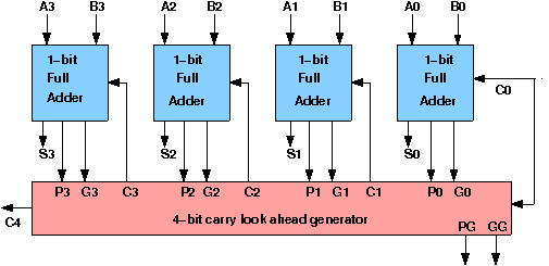
The number of gate levels for the carry propagation can be found from the circuit of full adder. The signal from input carry Cin to output carry Cout requires an AND gate and an OR gate, which constitutes two gate levels. So if there are four full adders in the parallel adder, the output carry C5 would have 2 X 4 = 8 gate levels from C1 to C5. For an n-bit parallel adder, there are 2n gate levels to propagate through.
Design Issues :
The corresponding boolean expressions are given here to construct a carry lookahead adder. In the carry-lookahead circuit we ned to generate the two signals carry propagator(P) and carry generator(G),
Pi = Ai ⊕ Bi
Gi = Ai · Bi
The output sum and carry can be expressed as
Sumi = Pi ⊕ Ci
Ci+1 = Gi + ( Pi · Ci)
Having these we could design the circuit. We can now write the Boolean function for the carry output of each stage and substitute for each Ci its value from the previous equations:
C1 = G0 + P0 · C0
C2 = G1 + P1 · C1 = G1 + P1 · G0 + P1 · P0 · C0
C3 = G2 + P2 · C2 = G2 P2 · G1 + P2 · P1 · G0 + P2 · P1 · P0 · C0
C4 = G3 + P3 · C3 = G3 P3 · G2 P3 · P2 · G1 + P3 · P2 · P1 · G0 + P3 · P2 · P1 · P0 · C0

Objective of 4 bit carry lookahead adder:
It computes the carries parallely thus greatly speeding up the computation.
- understanding behaviour of carry lookahead adder from module designed by the student as part of the experiment
- understanding the concept of reducing computation time with respect of ripple carry adder by using carry generate and propagate functions
- the adder wil add two 4 bit numbers
Examining behaviour of carry lookahead adder for the module designed by the student as part of the experiment (refer to the circuit diagram)
Loading data in the carry lookahead adder (refer to procedure tab for further detail and experiment manual for pin numbers)
- load the two input numbers in the adder units as:
- 1111 and 0001
Examining the carry generate and propagate function behaviour:
- check output sum 0000
- check final output carry 1
- check intermediate carry bit and sum bit of the unit adders and verify the values of carry generate and propagate function (refer to theory)
- probing the any port can be done by verifying the color of the wire coming out of the port
Recommended learning activities for the experiment: Leaning activities are designed in two stages, a basic stage and an advanced stage. Accomplishment of each stage can be self-evaluated through the given set of quiz questions consisting of multiple type and subjective type questions. In the basic stage, it is recommended to perform the experiment firstly, on the given encapsulated working module, secondly, on the module designed by the student, having gone through the theory, objective and procuder. By performing the experiment on the working module, students can only observe the input-output behavior. Where as, performing experiments on the designed module, students can do circuit analysis, error analysis in addition with the input-output behavior. It is recommended to perform the experiments following the given guideline to check behavior and test plans along with their own circuit analysis. Then students are recommended to move on to the advanced stage. The advanced stage includes the accomplishment of the given assignments which will provide deeper understanding of the topic with innovative circuit design experience. At any time, students can mature their knowledge base by further reading the references provided for the experiment.
- if value is UNKNOWN, wire color= maroon
- if value is TRUE, wire color= blue
- if value is FALSE, wire color= black
- if value is HI IMPEDENCE, wire color= green
- if value is INVALID, wire color= orange
Test plan:
- Set one input to zero(0) and check the output.
- Set one input to all one and another as 0001 in carry lookahead adder.
- Check the carry lookahead adder with two arbritrary input. Check the output and show the carry propagator and generator output for every bit.
Use Display units for checking output. Try to use minimum number of components to build. The pin configuration of the canned components are shown when mouse hovered over a component.
Assignment Statements :
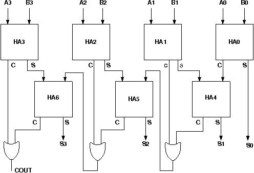
- Design a 4-bit carry lookahead adder circuit using half adders and full adders and test it by giving proper input.
- Design a 16-bit carry lookahead adder circuit using half adders and full adders and test it by giving proper input.

Design of Carry Lookahead Adders :
Procedure to perform the experiment:Design of Carry Lookahead Adders
- Start the simulator as directed.This simulator supports 5-valued logic.
- To design the circuit we need 7 half adder, 3 OR gate, 1 V+(to give 1 as input), 3 Digital display(2 for seeing input and 1 for seeing output sum), 1 Bit display(to see the carry output), wires.
- The pin configuration of a component is shown whenever the mouse is hovered on any canned component of the palette or press the 'show pinconfig' button. Pin numbering starts from 1 and from the bottom left corner(indicating with the circle) and increases anticlockwise.
- For half adder input is in pin-5,8 output sum is in pin-4 and carry is pin-1
- Click on the half adder component(in the Adder drawer in the pallet) and then click on the position of the editor window where you want to add the component(no drag and drop, simple click will serve the purpose), likewise add 6 more full adders(from the Adder drawer in the pallet), 3 OR gates(from Logic Gates drawer in the pallete), 1 V+, 3 digital display and 1 bit Displays(from Display and Input drawer of the pallet,if it is not seen scroll down in the drawer)
- To connect any two components select the Connection menu of Palette, and then click on the Source terminal and click on the target terminal. According to the circuit diagram connect all the components, connect V+ to the upper input terminals of 2 digital displays according to you input. connect the OR gates according to the diagram shown in the screenshot connect the pin-1 of the half adder which will give the final carry output. connet the sum(pin-4) of those adders to the terminals of the third digital display which will give output sum. After the connection is over click the selection tool in the pallete.
- See the output, in the screenshot diagram we have given the value 0011(3) and 0111(7) so get 10 as sum and 0 as carry.you can also use many bit switches instead of V+ to give input and by double clicking those bit switches can give different values and check the result.
Circuit diagram of Carry Lookahead Adder:
Components :
The components needed to create 4 bit carry lookahead adder is listed here -
- 7 half-adders: 4 to create the look adder circuit, and 3 to evaluate Si and Pi · Ci
- 3 OR gates to generate the next level carry Ci+1
- wires to connect
- LED display to obtain the output

Design of Carry Lookahead Adders :
General guideline to use the simulator for performing the experiment:
- Start the simulator as directed. For more detail please refer to the manual for using the simulator
- The simulator supports 5-valued logic
- To add the logic components to the editor or canvas (where you build the circuit) select any component and click on the position of the canvas where you want to add the component
- The pin configuration is shown when you select the component and press the 'show pinconfig' button in the left toolbar or whenever the mouse is hovered on any canned component of palette
- To connect any two components select the connection tool of palette, and then click on the source terminal and then click on the the target terminal
- To move any component select the component using the selection tool and drag the component to the desired position
- To give a toggle input to the circuit, use 'Bit Switch' which will toggle its value with a double click
- Use 'Bit Display' component to see any single bit value. 'Digital Display' will show the output in digital format
- undo/redo, delete, zoom in/zoom out, and other functionalities have been given in the top toolbar for ease of circuit building
- Use start/stop clock pulse to start or stop the clock input of the circuit. Clock period can be set from the given 'set clock' button in the left toolbar
- Use 'plot graph' button to see input-output wave forms
- Users can save their circuits with .logic extension and reuse them
- After building the circuit press the simulate button in the top toolbar to get the output
- If the circuit contains a clock pulse input, then the 'start clock' button will start the simulation of the whole circuit. Then there is no need to again press the 'simulate' button
Software for conducting the experiment, as appropriate for your platform, may be downloaded via SOFTWARE
General guideline to use the Simulator Software for performing the experiments:
- Windows (64 bit)
- Java runtime environment is needed (may get from java.com)
- Install downloaded jre
- Right click on My Computer/This PC
- Select Properties
- Select Advanced System Settings
- Select Advanced tab
- Select Environment Variables
- Select Path under System Variables
- Click on Edit button
- In Variable value editor paste this at the start of the line
C:\Program Files\Java\< jdk_version >\bin; - Click Ok then Ok again
- Linux (64 bit)
- If you are using linux platform then click on links under 'Linux(32 bit)' or if you are using then click on links under 'Windows(32 bit)' to download the Simulator Software
- Linux(32 bit)
- Windows(32 bit)
Click here to download the 64 bit version of simulator
PATH needs to be set:
If your environment is properly set up, you may open by double clicking on the jar file, otherwise use the following command:
java -jar coldvl64Windows.jar
Click here to download the 64 bit version of simulator
Once the simulator is downloaded, open the command prompt, then go to the directory where you have saved it using cd command and then give the following command to run the simulator:
java -jar coldvl64Linux.jar
Click here to download the new version of simulator
Once the simulator is downloaded, open the command prompt, then go to the directory where you have saved it using cd command and then give the following command to run the simulator:
java -jar coaSimulatorNew.jar
Click here to download the new version of simulator
Once the simulator is downloaded, open the command prompt, then go to the directory where you have saved it using cd command and then give the following command to run the simulator:
java -jar SimulatorNew.jar

You can download the Manuals from below mentioned links

Design of Carry Lookahead Adders :
Basic stage
Multiple choice questions:
- What is the main difference between half-adders and full-adders?
- Which one of the following will give the sum of full adders as output?
- The MOST commonly used system for representing signed binary numbers is the
- The time required for a pulse to decrease from 90 to 10 per cent of its maximum value is called
- Odd parity of word can be conveniently tested by
Nothing basically; full-adders are made up of two half-adders
Full-adders can handle double digit numbers
Full-adders have a carry input capability
Half-adders can only handle single digit numbers
Three bit parity checke
Three point majority circuit
Three bit counter
Three bit comparator
2's-complement system
1's-complement system
10's-complement system
Sign-magnitude system
Propagation delay
Rise time
Decay time
Binary level transition period
AND gate
OR gate
XOR gate
NOR gate
Subjective questions:
- What is the reason for using look ahead carry adder?
- What is the number of gate levels for output carry in a parrel adder composed of 4 full adders?
- What is the number of gate levels to propagate through for an n-bit parallel adder?
Advanced stage
Multiple choice questions:
- What distinguishes the look-ahead-carry adder?
- The time and space complexity of carry look ahead adder are respctively
- The number of full and half-adders required to add 16-bit numbers is
- The MOST commonly used system for representing signed binary numbers is the
- Ripple carry delay is increased in carry-look-ahead adder
- Carry of a full adder is a symmetric function
It requires advance knowledge of the final answer
It is faster than a ripple-carry adder
It is slower than the ripple-carry adder
It is easier to implement logically than a full-adder
O(n), O(nlogn)
O(n), O(1)
O(n), O(n)
O(logn), O(nlogn)
1 half-adder, 5 full-adders
4 half-adders, 12 full-adders
8 half-adders, 8 full-adders
16 half-adders, 0 full-adders
2's-complement system
1's-complement system
10's-complement system
Sign-magnitude system
True
False
True
False
Subjective questions:
- What is the worst case delay of an n-bit carry look ahead adder?
- What is the advantage of carry look head adder over ripple carry adder?
- What is the generate and propagate functions expression at level-2?
- What is the number of additions in carry look head adder for adding m numbers?

Design of Carry Lookahead Adders :
References :
Books:
- Digital Logic and Computer Design - M. Morris Mano. Pearson Education - Prentice Hall.
- Digital Principles Foundation of Circuit Design and Application - Arun Kumar Singh. New Age Publishers.
- The Art of Electronics - Paul Horowitz and Winfield Hill (1989). Cambridge University Press
- Modern Dictionary of Electronics - Rudolf F. Graf (1999). Newnes
Web Sites:
