
Bipolar Junction Transistors (BJTs)
What are BJTs?

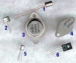
Bi-polar transistors are amongst the most widely used devices for amplification of all types of electrical signals in discrete circuits, (circuits made from individual components rather than integrated circuits). They are also used in circuits together with I/Cs since it is often more practical in circuits where large power or high voltage is needed to use discrete output transistors, while using low voltage, low power I/Cs for most of the signal processing. It is also often more convenient to use a discrete transistor for an individual circuit within a larger system for which integrated circuits are not readily available. For example an integrated circuit may carry out all of the processing of the signals in a system but then pass the processed signal to a single discrete transistor for power amplification to drive a loudspeaker. Transistors come in many shapes and types. A selection of typical transistors is shown in Fig 2.1.1
Fig. 2.1.1 Typical Bipolar Transistors
-
1. AC127
Germanium audio output transistor - found in vintage radios, and in some more modern circuits where sensitivity to heat is required. -
2. BF318
Silicon Video amplifier transistor uses a collector/emitter voltage (VCEO) of about 150V and will amplify frequencies up to 80MHz -
3. BU208A
Silicon output transistor use in TVs and large screen monitors. Can deliver high power and withstand pulse VCEO voltages of about 1000V. The metal case (normally bolted to a heat sink) is the collector connection. -
4. BD124
Silicon TV output transistor wth a lower power rating. -
5. BC108
General-purpose Silicon voltage amplifier transistor; the silver case with a small tab to identify the emitter connection is a standard TO39 package. -
6. BD 131
Silicon audio NPN output transistor in a TO26 package for mounting on a suitable heat sink; will dissipate 15W and is often used as part of a push-pull pair with a matched BD132 PNP transistor.

How a BJT (Bipolar Junction Transistor) Works
Its all in the doping
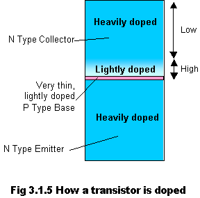

The way a transistor works can be described with reference to fig 3.1.5 which shows the basic doping of a junction transistor and Fig 3.1.6 the method of operation of the device.
The operation of the transistor is very dependant on the degree of doping of the various parts of the semiconductor crystal. The N type emitter is very heavily doped to provide many free electrons as majority charge carriers. The P type base region is extremely thin and the N type collector is very heavily doped to give it a low resistivity apart from a layer of less heavily doped material near to the base region. This change in the resistivity of the collector close to the base ensures that a large potential is present within the collector material close to the base. The importance of this will become apparent from the following description.
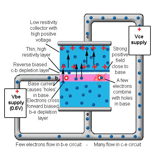
Fig. 3.1.6 How a Transistor Amplifies Current.
Animation ----->>Please click here to open BIPOLAR TRANSISTOR OPERAION Animation Window
During normal operation, a potential is applied across the base/emitter junction so that the base is approximately 0.6v more positive than the emitter, this makes the base/emitter junction forward biased.
A much higher potential is applied across the base/collector junction with a relatively high positive voltage applied to the collector so that the base/collector junction is heavily reverse biased. This makes the depletion layer between base and collector quite thick once power is applied.
As mentioned above, the collector is made up of mainly low resistivity material with a layer of high resistivity material next to the base/collector junction. This means that most of the voltage between collector and base is developed across this high resistivity layer, giving a high voltage gradient near the collector base junction.
When the base emitter junction is forward biased, a small current will flow into the base. Thus holes are injected into the P type material. These holes attract electrons across the forward biased base/emitter junction to combine with the holes. However, because the emitter region is very heavily doped, many more electrons cross into the base region than are able to combine with holes. Thus there is a large concentration of electrons in the base region and most of these electrons are swept straight through the very thin base, and into the base/collector depletion layer. Once here they come under the influence of the strong electric field across the base/collector junction. This field is so strong due to the potential gradient in the collector material mentioned earlier, that the electrons are swept across the depletion layer and into the collector material, and so towards the collector terminal.
Varying the current flowing into the base affects the number of electrons attracted from the emitter. In this way we can vary the large current flowing from emitter to collector by only tiny changes in the much smaller base current. Small changes in base current thus cause large changes in collector current, so current amplification is taking place and we can say that the transistor is a current amplification device.

A BJT is a Current Operated Transistor.
The current flowing between emitter and collector of a transistor is much greater than that flowing between base and emitter. Thus a small base current is controlling the emitter collector current. The ratio of the two currents, ICE/IBE is constant, provided that the collector emitter voltage Vce is constant. Therefore, if the base current rises, so does collector current.
This ratio is the CURRENT GAIN of the transistor and is given the symbol hfe. A fairly low gain transistor might have a current gain of 20 to 50, while a high gain type may have a gain of 300 to 800 or more. The spread of values of hfe for any given transistor is quite large, even in transistors of the same type and batch.
 The graph of ICE/IBE shown in fig 3.1.7 is called the
TRANSFER CHARACTERISTIC and the slope of the graph shows us the hfe for that
transistor.
The graph of ICE/IBE shown in fig 3.1.7 is called the
TRANSFER CHARACTERISTIC and the slope of the graph shows us the hfe for that
transistor.
Characteristic curves (graphs) can be drawn to show other parameters of a transistor and are used both to detail the performance of a particular device and as an aid to the design of amplifiers.
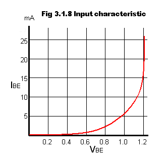
Fig 3.1.8, the INPUT CHARACTERISTIC shows a graph of base emitter current IBE against base emitter voltage VBE (IBE/VBE). This shows the input CONDUCTANCE of the transistor. As conductance I/V is the reciprocal of RESISTANCE (V/I) we can use this curve to determine the input resistance of the transistor. The steepness of this particular curve when the VBE is above 1 volt tells us that the input conductance is very high and there is a large increase in current (in practice, usually enough to destroy the transistor!)for a very small increase in VBE. Thus the input RESISTANCE must be low. Around 0.6 - 0.7 volts the graph curves shows that the input resistance of a transistor varies, according to the amount of base current flowing and below about 0.5 volts base current ceases.
Fig 3.1.9 shows the OUTPUT CHARACTERISTIC whose slope gives the value of output conductance (and by implication output resistance). The near horizontal parts of the graph lines show that a change in collector emitter voltage VCE has almost no effect on collector current in this region, just the effect we would expect if the transistor output had a large value resistor in series with it. Therefore we can say that the output resistance is high.
Thus, these graphs show that, for a silicon transistor with an input applied between base and emitter, and output taken between collector and emitter (a method of connection called common emitter mode) we would expect;

- Low input resistance (from the input characteristic).
- Fairly high gain (from the transfer characteristic)
- High output resistance (from the output characteristic)
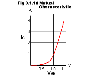
Fig 3.1.10 shows the graph of MUTUAL CONDUCTANCE IC/VBE and illustrates the change in collector current which takes place for a given change in base emitter voltage. (ie input signal voltage). This graph is for a typical silicon power transistor. Notice the large collector currents possible, and the nearly linear relationship between the input voltage and output current.
The characteristics described on this page are those relating to a typical power transistor connected in the "common emitter" mode. This is one of three possible modes of connection for a transistor.
Note: In many transistors the currents will be much smaller than shown here. For small signal amplifiers base currents will be a few micro-amps rather than milli-amps.